Tech Blog: Pushing the Envelope of Chip-to-Chip Communication

| Watch the new episode of Invented Arizona, where Kathleen Melde gives us a closer look at her invention.
|
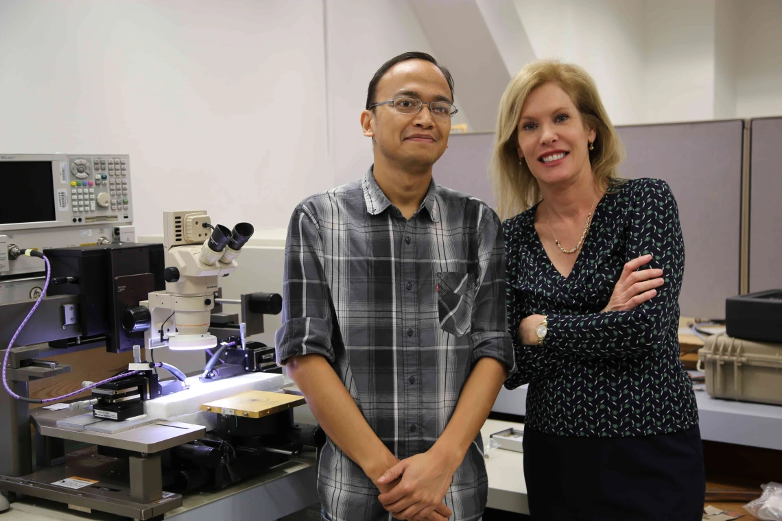
Funded by the US National Science Foundation, Kathleen Melde, PhD, professor and Prabhat Baniya, PhD candidate, at the University of Arizona Department of Electrical and Computer Engineering have created a chip-level “add-on” module that enables (multi-core) chip-to-chip wireless communication using reconfigurable antennas. Comparing her lab’s invention to that of how ants move large objects as a team, Melde described her small chips are similarly able to communicate large amounts of data by working together as a team.
We had the opportunity to get an inside look at Dr. Melde’s lab, where she explained the importance and benefits of her wireless chip.
TLA: Tell us about the background of your invention.
Melde: We created a very small antenna that can be mounted on silicon chips. The antenna allows us to use wireless links to connect to other antennas on other nearby chips. The antennas are used to transfer data so that the chips can share the computing workload. The technology is often called NoC (Network-on-a-Chip). We essentially created a dynamic local wireless network on a set of computer chips using reconfigurable antennas for on-chip computing. We are different from other antenna technologies because our antennas transfer data between chips that are in the same plane or are on the same layer.
TLA: What problem does it solve?
Melde: The problem is one that we face in multicore computing. It’s quite similar to parallel computer processing, but on a chip level. The solution eliminates some wirebonds and creates a wireless link. Also, some of the losses (due to the loss in the wires that make connections between chips) are reduced. And finally, if a link breaks, we can actually adapt or redirect the antenna beams around the broken links. This is not possible with wired connections, because such connections are fixed.
TLA: Who would be the top beneficiaries of a technology like this?
Melde: Generally industries designing systems and systems of sensors and computer would be the top beneficiaries.
TLA: What are you most excited about as you take this technology forward?
Melde: Now that we have the antenna technology, we plan on linking this to modules to demonstrate the quality of the data transfers. The good thing is that some of the simulation modules are so accurate that we can run simulations ahead of time to emulate real-time data transfers. Although we are excited to build and test, it is time consuming and costly. Running simulations ahead of time allow us to use our build/test approach very carefully and strategically.
I am also excited about scaling up the technology. We are planning on adding in more beam positions to be able to communicate with more chips; we’re targeting communications between eight neighboring chips, as opposed to the 4 diagonals now. Again, we are very confident of our design methodology and simulation accuracy. Having the validation of simulation and tests are always confirmation of the approaches and potential upscaling.
Interested in learning more about this invention? Would you like to talk to us about licensing opportunities? Visit the link below for details and contact information.
UA18-204: Chip-to-Chip Switched Beam Antenna Array with Integrated Feed Network(link is external)
Also, check out these related technologies:
- UA14-104: A Fault Tolerant and Power Efficient Network-on-Chip Architecture using Quad-Function Channel (QFC) Buffers(link is external)
- UA16-054: Methods for Securing Wireless Communications at the Physical Layer(link is external)

